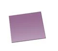
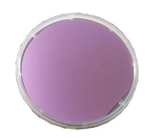
Thermal Oxide Wafer: 300 nm SiO2 Layer on Si (111), 3"dia x 0.50 mm t, N-type ,P-doped 1SP R:5-15 ohm.cm
Thermal Oxide Wafer: 300 nm SiO2 Layer on Si (111), 3"dia x 0.50 mm t, N-type ,P-doped 1SP R:5-15 ohm.cm
Thermal oxide Layer
-
Research Grade , about 80 % useful area
- SiO2 layer on 3" Silicon wafer
- Oxide layer thickness: 300 nm ( 3000A) +/-10%
- Refractive index - 1.455
Silicon Wafer Specifications:
- Conductive type: N-type/ P-dped
- Resistivity: 5-15 ohm.cm (If you would like to measure the resistivity accurately,
please order our Portable 4 Probe Resistivity Testing Instrument.) - Size: 3" +/- 0.5 mm in diameter x 0.5 mm +/- 0.05 mm th
- Orientation: (111) +/- 1o
- Polish: one side polished
- Surface roughness, Ra: < 5A (RMS)
-
Optional: you may need tool below to handle the wafer ( click picture to order )


Diamond Scriber for Cutting Single Crystal Substrate - DS-01
Micro-Fiber & Dust Free Wiper, 4"x4", 100 pcs/bag - Wiper-yx-2001
Vacuum Pen SMT-150C (NEW) - EQ-SMT-150C
Single Wafer Containers
Related Products
 |
|
|
|
|
|
Thin Films A-Z |
Crystal wafer A-Z |
Plasma Cleaner |
Wafer Containers |
Dicing saw |
Film Coater |
Product Information
Product Information
Shipping & Returns
Shipping & Returns
Description
Thermal oxide Layer
-
Research Grade , about 80 % useful area
- SiO2 layer on 3" Silicon wafer
- Oxide layer thickness: 300 nm ( 3000A) +/-10%
- Refractive index - 1.455
Silicon Wafer Specifications:
- Conductive type: N-type/ P-dped
- Resistivity: 5-15 ohm.cm (If you would like to measure the resistivity accurately,
please order our Portable 4 Probe Resistivity Testing Instrument.) - Size: 3" +/- 0.5 mm in diameter x 0.5 mm +/- 0.05 mm th
- Orientation: (111) +/- 1o
- Polish: one side polished
- Surface roughness, Ra: < 5A (RMS)
-
Optional: you may need tool below to handle the wafer ( click picture to order )
Diamond Scriber for Cutting Single Crystal Substrate - DS-01
Micro-Fiber & Dust Free Wiper, 4"x4", 100 pcs/bag - Wiper-yx-2001
Vacuum Pen SMT-150C (NEW) - EQ-SMT-150C
Single Wafer Containers
Related Products
|
|
|
|
|
|
Thin Films A-Z |
Crystal wafer A-Z |
Plasma Cleaner |
Wafer Containers |
Dicing saw |
Film Coater |