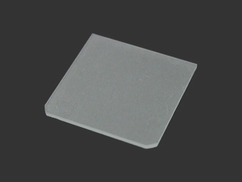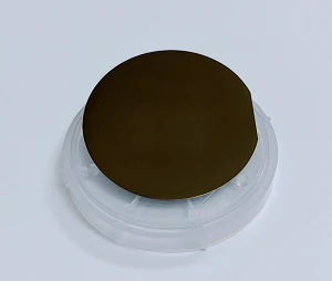

GaN Single Crystal Substrate,N-type, (10-10), 5 x10 x 0.3 mm , 1SP
GaN single crystal substrates is made by a hydride vapor phase epitaxy (HVPE)-based method. During the HVPE process, HCl reacts with molten Ga to form GaCl, which in turn reacts with NH3 to form GaN. The large growth rate enables the growth of self-supporting wafer thicknesses in a convenient time period.
Specifications of Substrate
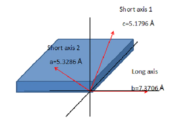
- Orientation: M-axis (10-10) +/- 1.0 o
- Type: N-type(undoped)
- Nominal Thickness 300+/- 25 microns
- Dimension: 5 mm x 10 mm +/- 0.5 mm
-
Resistivity <0.5 ohm.cm
- Dislocation Density < 5x10^5 cm^-2
- TTV: <=15 um
- BOW: <=20 um
- Front Surface Finish (Ga Face) , RMS <2.0 nm, Epi-Ready polished
- Back Sutface Finish: Fine Ground
- Useable Surface area: >90%
- Package Single Wafer Container or membrane box
- For XRD & AFM data, please click here
Related Products
Other Sapphire |
GaN |
AlN template |
ZnO |
|
|
|
|
Diamond Scriber |
Vacuum Pen |
Wafer Containers |
Film Coaters |
|
|
|
|
Original: $909.00
-65%$909.00
$318.15Product Information
Product Information
Shipping & Returns
Shipping & Returns
Description
GaN single crystal substrates is made by a hydride vapor phase epitaxy (HVPE)-based method. During the HVPE process, HCl reacts with molten Ga to form GaCl, which in turn reacts with NH3 to form GaN. The large growth rate enables the growth of self-supporting wafer thicknesses in a convenient time period.
Specifications of Substrate
- Orientation: M-axis (10-10) +/- 1.0 o
- Type: N-type(undoped)
- Nominal Thickness 300+/- 25 microns
- Dimension: 5 mm x 10 mm +/- 0.5 mm
-
Resistivity <0.5 ohm.cm
- Dislocation Density < 5x10^5 cm^-2
- TTV: <=15 um
- BOW: <=20 um
- Front Surface Finish (Ga Face) , RMS <2.0 nm, Epi-Ready polished
- Back Sutface Finish: Fine Ground
- Useable Surface area: >90%
- Package Single Wafer Container or membrane box
- For XRD & AFM data, please click here
Related Products
Other Sapphire |
GaN |
AlN template |
ZnO |
|
|
|
|
Diamond Scriber |
Vacuum Pen |
Wafer Containers |
Film Coaters |
|
|
|
|