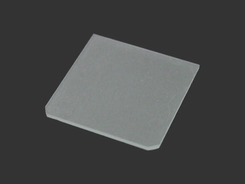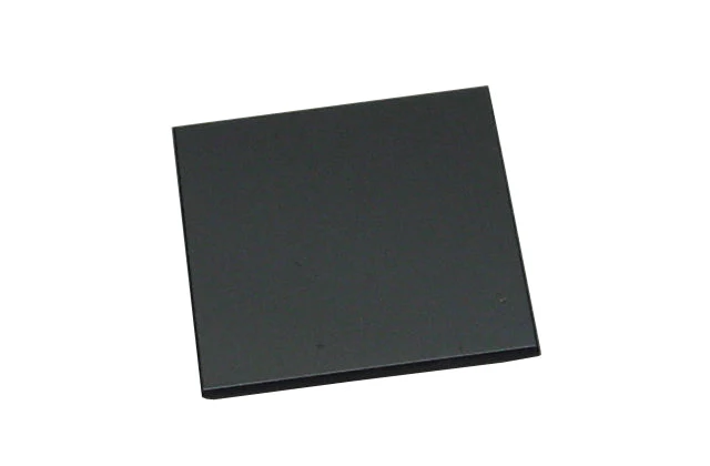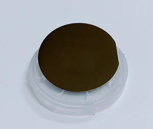

GaP Wafer, Undoped (111) 10x10x0.35 mm, 2sp - GPUc1010035S2
- GaP single crystal wafer,
- Size: 10mm x 10 mm x 0.35 mm,
- Doping: undoped,
- Conducting type: N-type,
- Orientation: (111)
- Polished: Two sides
- Surface finish (RMS or Ra) :: < 8A
- price is for one piece
Typical Physical Properties |
||
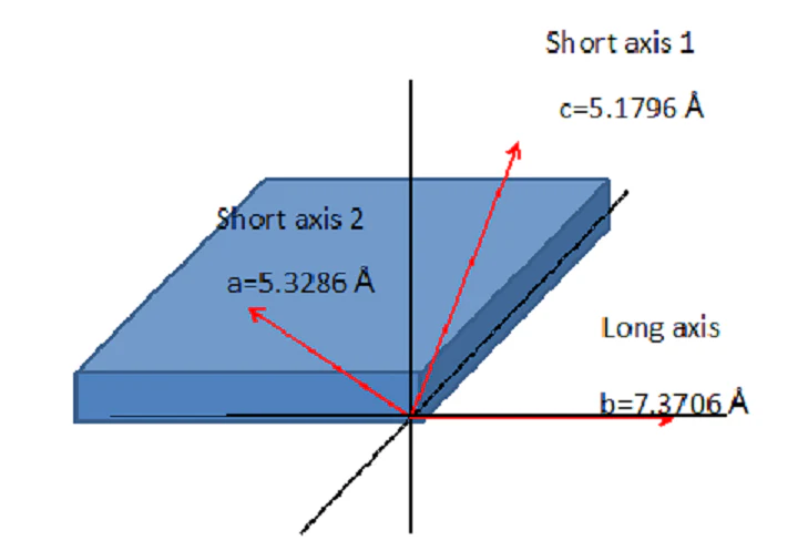
Crystal Structure |
Cubic. a =5.4505 Å |
|
Growth Method |
CZ (LEC) |
|
Density |
4.13 g/cm3 |
|
Melt Point |
1480 oC |
|
Thermal Expansion |
5.3 x10⁻⁶ / oC |
|
Dopant |
S doped |
undoped |
Crystal growth axis |
<111> or <100> |
<100> or <111> |
Conducting Type |
N |
N |
Carrier Concentration |
2 ~ 8 x10¹⁷ /cm3 |
4 ~ 6 x10¹⁶ /cm3 |
Resistivity |
~ 0.03 W-cm |
~ 0.3 W-cm |
EPD |
< 3x10⁵ |
< 3x10⁵ |
|
|
|
|
|
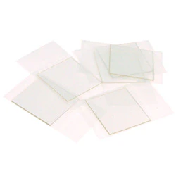
Other Crystal wafer A-Z |
Plasma Cleaner |
Wafer Containers |
Dicing saw |
Film Coater |
Original: $185.00
-65%$185.00
$64.75Product Information
Product Information
Shipping & Returns
Shipping & Returns
Description
- GaP single crystal wafer,
- Size: 10mm x 10 mm x 0.35 mm,
- Doping: undoped,
- Conducting type: N-type,
- Orientation: (111)
- Polished: Two sides
- Surface finish (RMS or Ra) :: < 8A
- price is for one piece
Typical Physical Properties |
||
Crystal Structure |
Cubic. a =5.4505 Å |
|
Growth Method |
CZ (LEC) |
|
Density |
4.13 g/cm3 |
|
Melt Point |
1480 oC |
|
Thermal Expansion |
5.3 x10⁻⁶ / oC |
|
Dopant |
S doped |
undoped |
Crystal growth axis |
<111> or <100> |
<100> or <111> |
Conducting Type |
N |
N |
Carrier Concentration |
2 ~ 8 x10¹⁷ /cm3 |
4 ~ 6 x10¹⁶ /cm3 |
Resistivity |
~ 0.03 W-cm |
~ 0.3 W-cm |
EPD |
< 3x10⁵ |
< 3x10⁵ |
|
|
|
|
|
Other Crystal wafer A-Z |
Plasma Cleaner |
Wafer Containers |
Dicing saw |
Film Coater |