✨ New Arrivals Just Dropped!Explore


InP, Growing Method: VGF(100) Zn doped,3 " x 0.625mm, wafer, 1sp
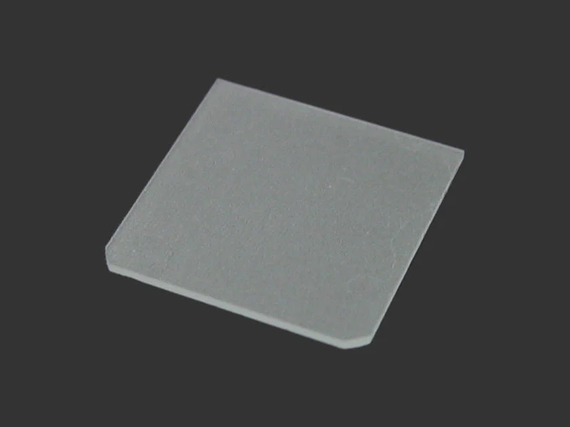
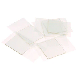
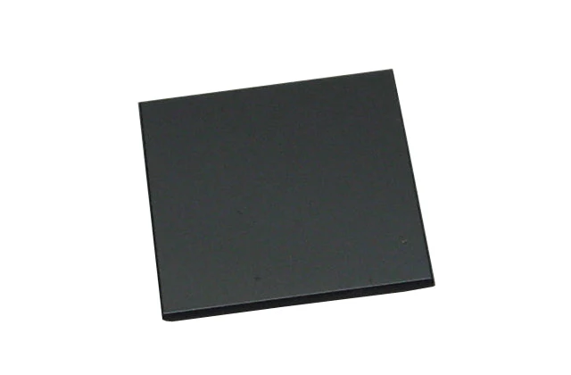
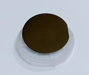
InP single crystal wafer
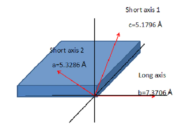
Orientation: (100)+/- 0.5 degree
Primary Flat: US(01-1)+/-0.5 degree
Secondary Flat: US(011)
Size: 3" diameter x 0.625 mm
Orientation: (100)+/- 0.5 degree
Primary Flat: US(01-1)+/-0.5 degree
Secondary Flat: US(011)
Size: 3" diameter x 0.625 mm
Growing Method: VGF
Doping: Zn doped
Conducting type: S-C
Polish: one side polished
Doping: Zn doped
Conducting type: S-C
Polish: one side polished
Resistivity: (4.19-4.73)E-2 ohm.cm
Mobility: 72-74 cmE2/V.S
EPD: <5000 /cmE2Carrier
Concerntration: (1.79-2.07)E18 /cmE-3
Ra(Average Roughness) : < 0.4 nm
EPD: <5000 /cmE2Carrier
Concerntration: (1.79-2.07)E18 /cmE-3
Ra(Average Roughness) : < 0.4 nm
EPI ready surface and packing
$2,515.00
InP, Growing Method: VGF(100) Zn doped,3 " x 0.625mm, wafer, 1sp—
$2,515.00
Product Information
Product Information
Shipping & Returns
Shipping & Returns
Description
InP single crystal wafer
Orientation: (100)+/- 0.5 degree
Primary Flat: US(01-1)+/-0.5 degree
Secondary Flat: US(011)
Size: 3" diameter x 0.625 mm
Orientation: (100)+/- 0.5 degree
Primary Flat: US(01-1)+/-0.5 degree
Secondary Flat: US(011)
Size: 3" diameter x 0.625 mm
Growing Method: VGF
Doping: Zn doped
Conducting type: S-C
Polish: one side polished
Doping: Zn doped
Conducting type: S-C
Polish: one side polished
Resistivity: (4.19-4.73)E-2 ohm.cm
Mobility: 72-74 cmE2/V.S
EPD: <5000 /cmE2Carrier
Concerntration: (1.79-2.07)E18 /cmE-3
Ra(Average Roughness) : < 0.4 nm
EPD: <5000 /cmE2Carrier
Concerntration: (1.79-2.07)E18 /cmE-3
Ra(Average Roughness) : < 0.4 nm
EPI ready surface and packing