✨ New Arrivals Just Dropped!Explore

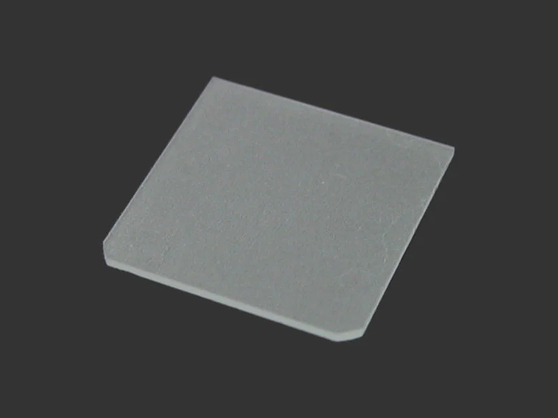
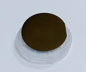
Silicon-on-Sapphire (11-02, R Plane ), 10mmx 10mmx0.46mm,2sp, Film: 1.0 um thick
Silicon on sapphire (SOS) is a hetero-epitaxialprocess for integrated circuitmanufacturing that consists of a thin layer (typically thinner than 0.6 micrometres) of silicongrown on a sapphire (Al2O3) wafer. SOS is part of the Silicon on Insulator (SOI) family of CMOS technologies. SOS is primarily used in aerospace and military applications because of its inherent resistance to radiation.
Materials: Silicon on Sapphire
Materials: Silicon on Sapphire
Silicon EPI Layer:
-
Silicon Orientation: (100)
-
Type, Dopant: Intrinsic type, undoped
-
Silicon Thickness: 1.0 um +/- 10%
-
Resistivity: > 100 ohm.cm
-
Micro-particle density ( for particles > 2 um) < 2/cm^2
Sapphire Wafer:
-
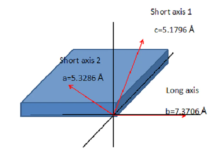
R plane -- (1-102) with single flat
-
Wafer size: 10x10 x 0.46 mm thickness
-
Front surface: Epi-polished (Ra < 4 nm)
-
Back surface: Optical grade polish
-
TTV < 15 um, Bow < 20 um, Warp < 20 um, Flatness (TIR) < 12 um
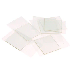
Related Products
 |
|
|
|
|
|
|
Thin Films A-Z |
Crystal wafer A-Z |
Plasma Cleaner |
Wafer Containers |
Dicing saw |
Film Coater |
$149.00
Silicon-on-Sapphire (11-02, R Plane ), 10mmx 10mmx0.46mm,2sp, Film: 1.0 um thick—
$149.00
Product Information
Product Information
Shipping & Returns
Shipping & Returns
Description
Silicon on sapphire (SOS) is a hetero-epitaxialprocess for integrated circuitmanufacturing that consists of a thin layer (typically thinner than 0.6 micrometres) of silicongrown on a sapphire (Al2O3) wafer. SOS is part of the Silicon on Insulator (SOI) family of CMOS technologies. SOS is primarily used in aerospace and military applications because of its inherent resistance to radiation.
Materials: Silicon on Sapphire
Materials: Silicon on Sapphire
Silicon EPI Layer:
-
Silicon Orientation: (100)
-
Type, Dopant: Intrinsic type, undoped
-
Silicon Thickness: 1.0 um +/- 10%
-
Resistivity: > 100 ohm.cm
-
Micro-particle density ( for particles > 2 um) < 2/cm^2
Sapphire Wafer:
-
R plane -- (1-102) with single flat
-
Wafer size: 10x10 x 0.46 mm thickness
-
Front surface: Epi-polished (Ra < 4 nm)
-
Back surface: Optical grade polish
-
TTV < 15 um, Bow < 20 um, Warp < 20 um, Flatness (TIR) < 12 um
Related Products
|
|
|
|
|
|
|
Thin Films A-Z |
Crystal wafer A-Z |
Plasma Cleaner |
Wafer Containers |
Dicing saw |
Film Coater |