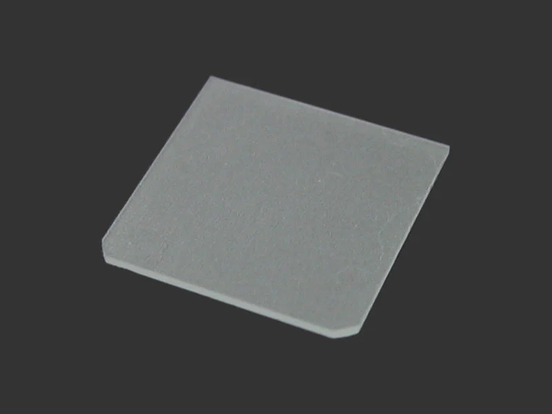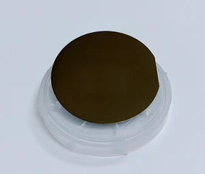

SOI Wafer: 6", 2.5 "m (P-doped ) + 1.0 SiO2 + 625um Si (P-type /Boron doped )
|
Device Layer |
||
|
Diameter: |
|
6" |
|
Type/Dopant: |
|
N type/P-doped |
|
Orientation: |
|
<1-0-0>+/-.5 degree |
|
Thickness: |
|
2.5±0.5µm |
|
Resistivity: |
|
1-4 ohm-cm |
|
Finish: |
Front Side Polished |
|
|
Buried Thermal Oxide: |
||
|
Thickness: |
|
1.0um +/- 0.1 um |
|
Handle Wafers: |
||
|
Type/Dopant |
P Type, B doped |
|
|
Orientation |
|
<1-0-0>+/-.5 degree |
|
Resistivity: |
|
10-20 ohm-cm |
|
Thickness: |
|
625 +/- 15 um |
|
Finish: |
|
As-received (not polished) |
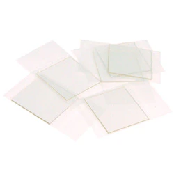
Related Products
 |
|
|
|
|
|
|
Thin Films A-Z |
Crystal wafer A-Z |
Plasma Cleaner |
Wafer Containers |
Dicing saw |
Film Coater |
Original: $329.00
-65%$329.00
$115.15Product Information
Product Information
Shipping & Returns
Shipping & Returns
Description
|
Device Layer |
||
|
Diameter: |
|
6" |
|
Type/Dopant: |
|
N type/P-doped |
|
Orientation: |
|
<1-0-0>+/-.5 degree |
|
Thickness: |
|
2.5±0.5µm |
|
Resistivity: |
|
1-4 ohm-cm |
|
Finish: |
Front Side Polished |
|
|
Buried Thermal Oxide: |
||
|
Thickness: |
|
1.0um +/- 0.1 um |
|
Handle Wafers: |
||
|
Type/Dopant |
P Type, B doped |
|
|
Orientation |
|
<1-0-0>+/-.5 degree |
|
Resistivity: |
|
10-20 ohm-cm |
|
Thickness: |
|
625 +/- 15 um |
|
Finish: |
|
As-received (not polished) |
Related Products
|
|
|
|
|
|
|
Thin Films A-Z |
Crystal wafer A-Z |
Plasma Cleaner |
Wafer Containers |
Dicing saw |
Film Coater |